File:Silicon wafer (Peellden).jpg
From NY Science Standards Wiki
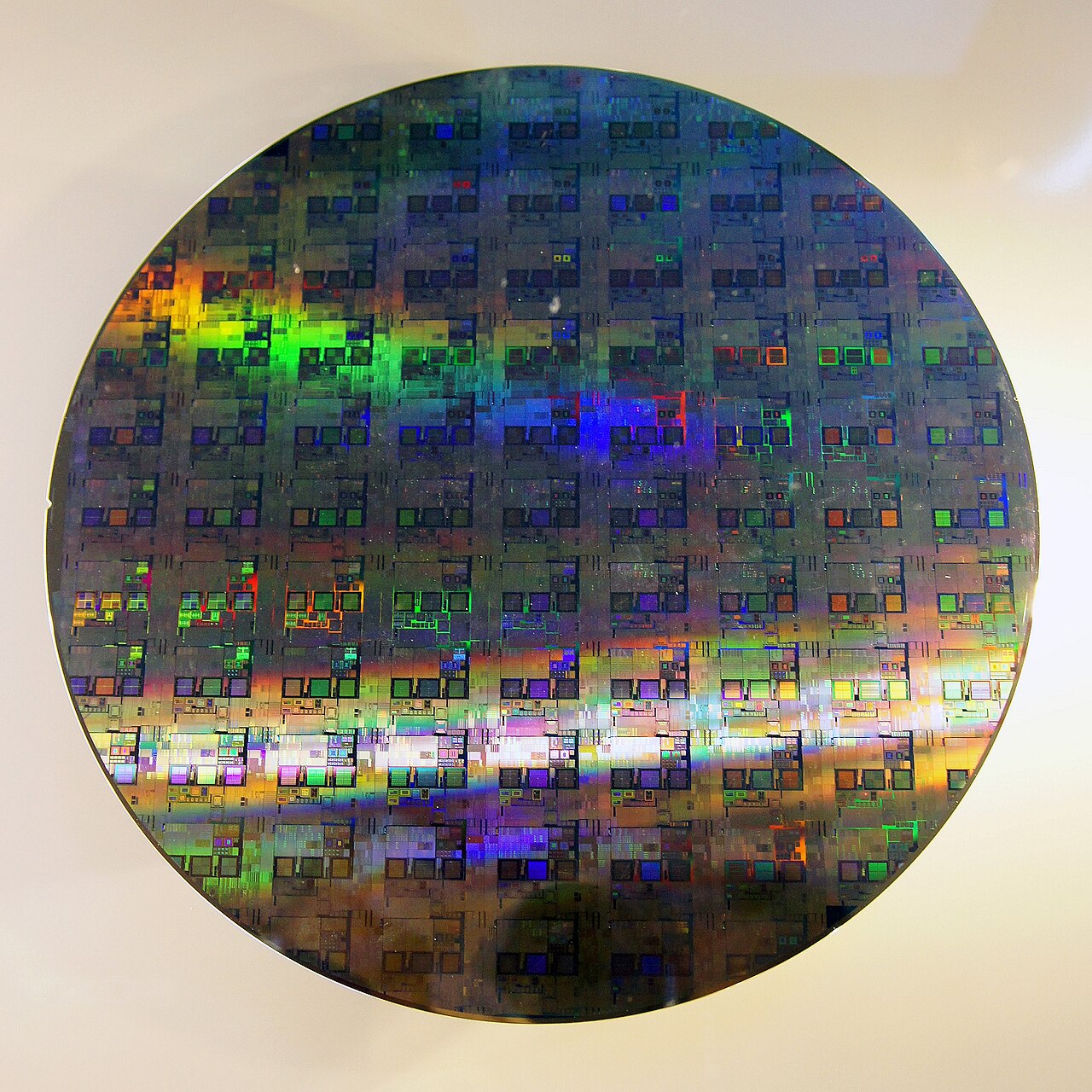
Size of this preview: 600 × 600 pixels. Other resolutions: 240 × 240 pixels | 1,280 × 1,280 pixels.
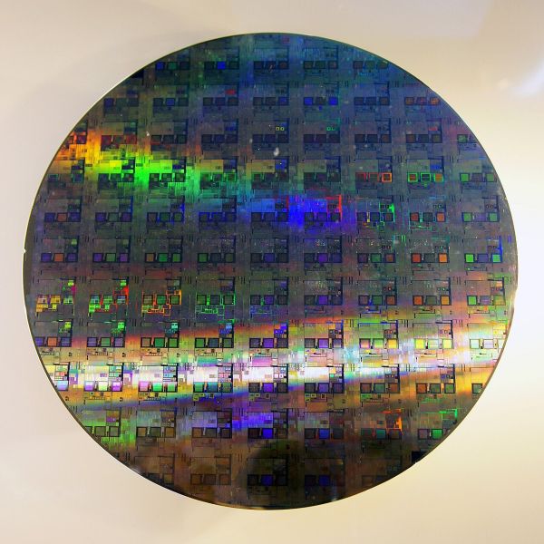
Original file (1,280 × 1,280 pixels, file size: 432 KB, MIME type: image/jpeg)
Summary
A 12-inch silicon wafer patterned with integrated circuits. Used on HS-PS2-6 to illustrate doped silicon semiconductors.
Source: Wikimedia Commons, File:12-inch silicon wafer.jpg (1280 px version).

Author: Peellden.
Licensing
This file is licensed under the Creative Commons Attribution-Share Alike 3.0 license (CC BY-SA 3.0). Attribution: Peellden, via Wikimedia Commons.
File history
Click on a date/time to view the file as it appeared at that time.
| Date/Time | Thumbnail | Dimensions | User | Comment | |
|---|---|---|---|---|---|
| current | 01:31, 16 October 2026 | | 1,280 × 1,280 (432 KB) | Conrad (talk | contribs) | Upload from Wikimedia Commons (CC BY-SA 3.0, Peellden) for HS-PS2-6 phenomena gallery |
You cannot overwrite this file.
File usage
There are no pages that use this file.
